Sustainability
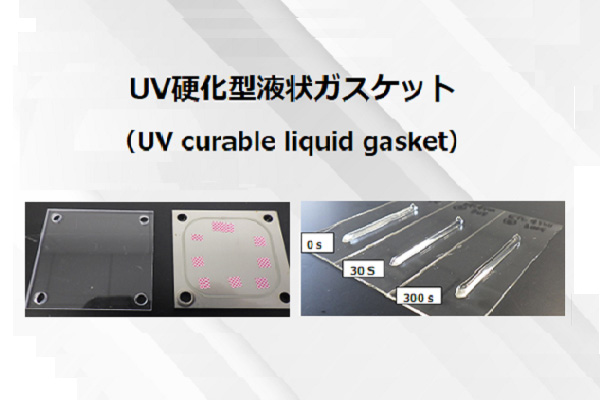
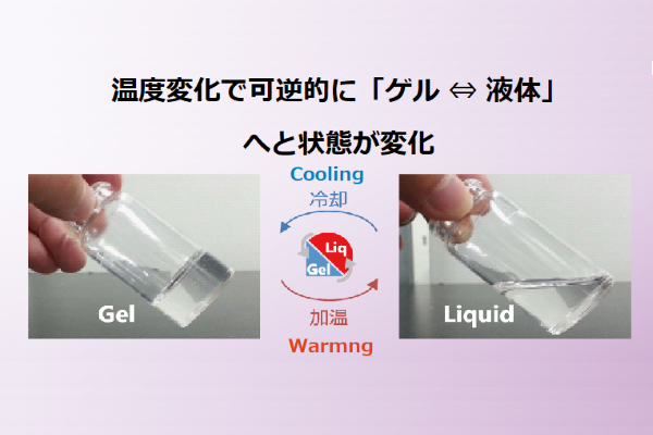
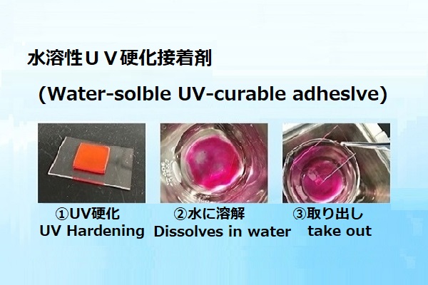
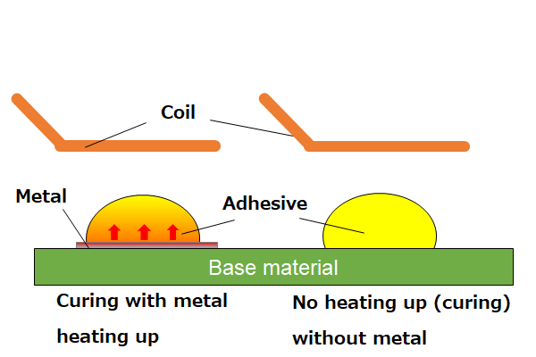
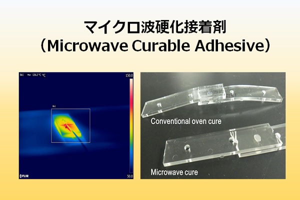
This technology achieves a sustainable society with solventless, low energy curing, and easy disassembly.
We introduce technologies created through Kyoritsu Chemical's research & development and related technical information.
This technology achieves a sustainable society with solventless, low energy curing, and easy disassembly.
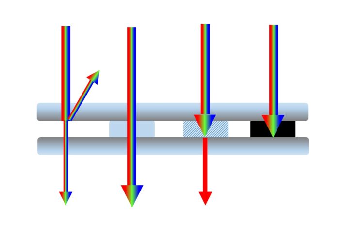
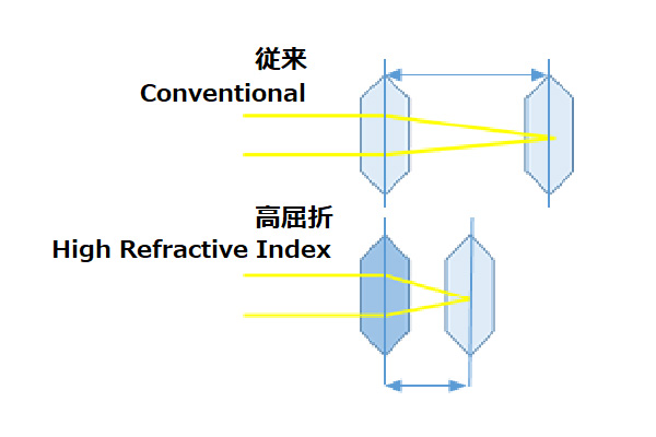
This technology controls the refraction and absorption of light by selecting optimum molecular structures. Diverse optical functions can be added, including a refractive index, Abbe’s number, birefringence, wavelength cutting, light shielding (OD), matte, reflection, and scattering.
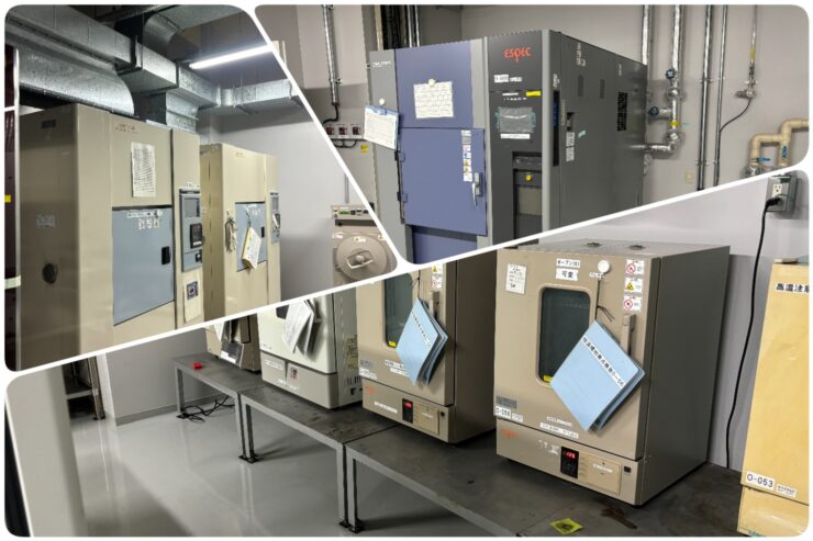
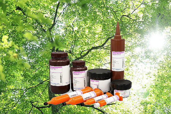
This technology is indispensable for applications used under harsh environments and applications expecting long-term use. Making full use of the molecular design and formulation design of materials, we contribute to quality improvements of products and services that our customers provide.